


| CERN -> ATLAS -> TU Vienna | ||
|
High-Density Digital Links | |
| signal generation |
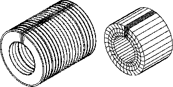
A charged particle traversing the straw ionizes the gas inside the straw along its path. Due to the high voltage of about 1,600 V which is maintained between the wall of the straw (cathode) and the wire (anode), the electrons generated in the ionization start to drift towards the wire and the ions to the wall of the straw - see Figure 2.2. The generated signal as seen in Figure 1.6 is a function of the drift velocity of the electrons and ions. The use of a Xe-gas mixture adds an unusual behavior compared to other cylindrical proportional chambers without Xe. For instance, complex processes occur near the wire like the creation of stable negative ions in an avalanche process [7].
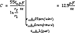
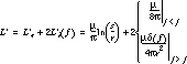
Electrically, the straw is a high-impedance current source. Its signal form contains a fast-electron component of about 3 to 5% of the total charge and a very-slow-ion component which adds a large tail of a duration of 60 us to the signal.
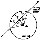 |
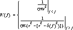
The electron component in Figure 1.6 can be calculated as a Gaussian impulse of 0.5-ns duration [7]. The ion current Iion is parametrized by complicated functions like
| signal transmission |
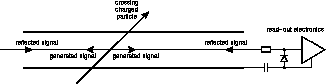
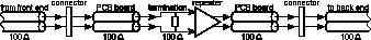
After the signal is generated it sees the straw as a transmission line to the read-out electronics and propagates in both direction of the straw - see Figure 2.3 If the straw is not properly terminated at its ends, the signal will be reflected and will create ghost images for the read-out electronics.
 |
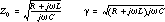
Coaxial structures like the straw have a characteristic impedance of

 and
and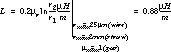 .
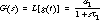
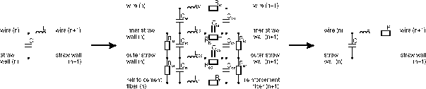
.A complete model of the straw consists of four lines: the wire, the inner and the outer wall of the straw, and the reinforcement fibre. Serial capacitors simulate the effect of the helical structure where one turn is not touching the next turn. The conductive glue between the inner and the outer wall of the straw and the random connection of the reinforcement fibre add additional parallel resistors. As the values of the components of this model change along the straw, the simulation of this model is very complex and not reasonable as most of the effects become merely important when the transmission line extensively extends in length.
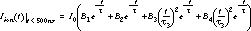
Including the losses of the straw into the model by a serial resistor of about 200 Ohm changes the characteristic properties to frequency-dependent values:
| termination |
The measurements mentioned above led the TRT collaboration to the conclusion to terminate the straw as transmission line only at the input of the readout electronics [8].
If the signal is generated at the near end of the straw close to the read-out electronics and the straw is not terminated at both ends, the signal will be reflected at the far end and generate a ghost image of the signal after the time

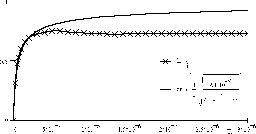
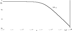
However, the read-out electronics has a peaking time of 8 ns and a shaping time of 20 ns. Thus the difference of the peaking time of the shaped signal from the particle crossing the near end of the straw and from a particle crossing at the far end is smaller than the timing resolution of 3.125 ns of the drift-time measurement - see Figure 2.5. Simulations and measurements [8] give a uniformity of the amplitude of the signal of better than 5%.
Thus signal integrity is provided when all straws are terminated at their read-out end by about 300 Ohm.
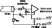
The minimum value of the decoupling capacitor CC is set to 100 pF to get a low impedance compared to the impedance of the straw and of the front-end electronics input for the times of interest of 5 to 20 ns. The maximum value is set by the input protection needed for the front-end electronics. In case of a discharge or spark in any straw in a group, the attached front-end-electronics chip will receive the energy stored in the straw capacitance (about 15 pF) and in the decoupling capacitor. Thus the maximal possible value for CC will be 1 nF (125 pF per straw). The final value has still to be investigated [14].
The protection network consists of a fast diode and a current-limiting resistor. Several configurations were tested [15]. The recent choice is a 1206-SMD resistor of 22 Ohm and a SMD diode. This limits a discharge with a rising time of about 30 ns and a total discharge time of about 2 us to a maximum amplitude of 10 V.
| signal transmission |
In terms of signal integrity, the protection network and the decoupling capacitor should not affect the signal as the first stage of the front-end electronics is a charge amplifier. Nevertheless, the network and the capacitor could cause additional reflections on the transmission line and have to be placed close to the read-out electronics. Physically the barrel and the end cap implement different solutions.
| barrel |
The straws of the barrel section are glued to the high-voltage board which is supplied with high-voltage by copper-plated kapton sheets. The wires are connected with pins to the tension plate which also provides the correct tension of the wires. The tension plate is a double-sided PCB board and routes the signal to the protection resistor, to the electronics boards, and back to the decoupling capacitor which is housed in a plastic sleeve and connects to the high-voltage plate - see Figure 2.7.
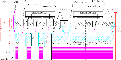 |
The signal directly flows from the anode of the straw to the wire pin, on the tension plate over the protection resistor to the connector for the read-out electronics back over the ground pins of this connector, the ground plane of the tension plate, and the decoupling capacitor to the HV-plate where it ends at the cathode of the straw. Each part of this path implies a discontinuity of the transmission line - the straw.
However, this path is very short compared to the wavelengths of the interesting frequencies. The signal will need only picoseconds to travel to the read-out electronics. The parasitic components of the path act like lumped components which are too small to interfere with the termination of the transmission line. Therefore they should not affect the integrity of the signal.
| end cap |
The straws of the end-cap section are connected to the read-out electronics with a flexible-rigid PCB board called the active web - Figure 2.8. Beside the electrical connections, it holds the components for the protection network, for the high-voltage distribution and the decoupling capacitor, and it provides, together with the carbon-fibre rings, structural stability for the end cap.
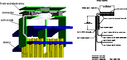 |
The signal from the wires passes along the inner flexible part of the active web, over the vertical rigid part to the horizontal rigid part where the protection network is situated. The horizontal rigid part of the active web also holds the connector to the read-out electronics. Back from the read-out electronics, the signal travels over the ground plane of the horizontal rigid part of the active web to the vertical part where the decoupling capacitor is placed, and back over the outer flexible HV layer to the straws.
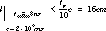
Like for the barrel section, it is essential for the end cap that the path from the straw to the read-out electronics is very short in order to not introduce additional reflections. But in contrast to the barrel, this signal path can reach a quite substantial length. Especially for wheel type B, the horizontal parts of the active web can reach up to 60 mm. The different characteristic impedances will add additional reflections - see Figure 2.9.
 |
The straw has a characteristic impedance of 300 Ohm - see chapter 2.1.1. The flexible part of the web is difficult to match to a certain impedance. The characteristic impedance for paired strips [17]
Nevertheless, the effect can be minimized by reducing the length of the signal path. The signal delay should not be longer than one tenth of the rise time of the read-out electronics (8 ns). Thus the whole path has to be kept shorter than
 .
.
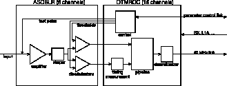 |
| ASDBLR |
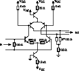
The ASDBLR (Amplifier-Shaper-Discriminator with BaseLine Restoration) is a full-custom, analogue, bipolar ASIC. It provides eight channels with amplifier, shaper, discriminator, and base-line restorer. It is largely a differential circuit which includes tail compensation and a capacitively-coupled, diode-clamped baseline restorer. Separate high- and low-sensitivity discriminators detecting charges of more than 50 fC and 1.5 fC, respectively, allow for both tracking and TR-photon detection on each channel.
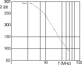
The input stage of the ASDBLR is a differential amplifier. Only one of the inputs is connected to the signal from the straws. The other input is connected to a dummy line on the printed-circuit board to stabilize the chip and to allow differential pickup-rejection techniques. Balancing the capacitive and resistive feedback allows control of the input impedance - see Figure 2.12.
 |
The output of the two discriminators is encoded into a programmable bi-level output current. - a ternary encoded differential signal distributed over two lines (true and complementary) - see Table 2.11 and Figure 2.13:
| amplified signal in the ASDBLR | true signal | complementary signal |
|---|---|---|
| no signal above thresholds | - 200 uA | - 600 uA |
| signal between low and high thresholds | - 400 uA | - 400 uA |
| signal above both thresholds | - 600 uA | - 200 uA |
 |
| DTMROC |
The DTMROC (Drift-Time Measurements ReadOut Chip) is a digital CMOS chip. It is a 16-channel device which provides drift-time measurement, pipeline, derandomizer, LVDS driver and receiver and a control section.
The DTMROC receives [19] the ternary encoded information from the ASDBLR, recovers the high and the low threshold signals, and samples the low threshold signal level every 1 / 8 of the cycle time - 3.125 ns. This information is stored and delayed in a memory - the pipeline. If an event is accepted, which is indicated by an external trigger signal (L1A), the corresponding data of three subsequent time slices is shifted into a derandomizer. Low-level differential drivers [20] with voltage swings between 50 mV and 400 mV transmit the formatted data to the back-end electronics. The swing is controlled by a bias current set by an external resistor and, when properly adjusted, is compatible with LVDS. The self-triggered readout starts as soon as possible after a trigger is received.
Low-voltage-differential receivers which are sensitive to voltage swings between 50 mV and 400 mV, receive the control signals - such as the clock and the trigger - from the back-end electronics. At the moment, the signals for the parameter control of the chip are standard CMOS-TTL signals with a clock frequency of 1 MHz. In the production version of the chip, these signals will also be low-level differential.
Furthermore, the DTMROC controls the ASDBLR by setting the thresholds. Two test-pulse circuits allow to test the ASDBLR by capacitively injecting test pulses to the inputs of the ASDBLR.
| ASTRAL |
The baseline is to integrate both chips into one design - the ASTRAL. The recent commercialisation of the DMILL semiconductor process [21] opens the possibility of combining the functionality of both devices on a single radiation-hard BiCMOS substrate. This would gain significant mounting area on the detector as no ternary driver and receiver would be necessary and both functions would be situated inside one single package. However, the ASTRAL will have a chip area of about 90 mm 2 which drastically reduces the yield of the production process.
| signal transmission |
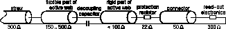
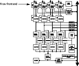
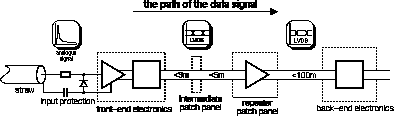
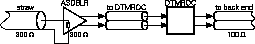
The signal transmission on the front-end electronics consists of three parts: the transmission to the ASDBLR, from the ASDBLR to the DTMROC, and from the DTMROC to the back-end electronics - see Figure 2.14.
As discussed in Chapter 2.1.1, the straws are terminated only at the electronics end. This is achieved at the input of the preamplifier - the input stage of the ASDBLR has been designed that it provides a good termination and minimizes the noise level by cutting off high frequencies - Figure 2.12. The traces to the inputs of the ASDBLR should be kept as short as possible - see Chapter 2.1.2.
The ternary receiver of the DTMROC receives the current steps of the ASDBLR into a low input impedance of 85 to 130 Ohm each side thereby avoiding excessive RC time constants due to stray capacitances on the input pins. The circuit is stable for input load capacitances as large as 50 pF but will have its optimal speed characteristics for an input load capacitance of less than 5 pF. The receiver is able to respond to a 4 ns input pulse of 200 uA. A 400-uA current pulse will be triggered if wider than 5 ns. Thus it is essential to keep the traces short and at the same length.
The output of the DTMROC is a low-voltage differential digital signal (LVDS) transmitting 40 Mbit per second with a simple protocol. The event data consists of 459 bit containing a 3-bit preamble "101", a header with status information, and the data of the 16 channels in three time slices (9 bit each). The drive current of the differential driver is programmable with an external resistor and can range from 0 to 8 mA. Thus the driver is able to drive a current of 3 mA at one line and sink it at the other line with a common DC level of 1.2 V when adjusted to the LVDS standard. This gives a differential voltage of ± 300 mV for a load of 100 Ohm. The PCB traces from the driver to the connector have to be adjusted to the wave impedance of the connected cable (~ 100 Ohm).
| barrel |
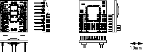
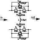
The printed-circuit boards of the different modules of the barrel and the end cap follow quite opposite design philosophies. The front-end electronics of the barrel consists of small daughter boards - also called stamp cards - see Figure 2.15.
The ASDBLR daughter board holding two ASDBLRs plugs directly into the tension plate of a module. Upon follows the DTMROC daughter board with one DTMROC. Two triangular roof boards - see Figure 2.16 - connect on top to a high number of DTMROC daughter boards to gather the signals together and to distribute the control signals and power.
 |
Each tension plate of the inner modules holds 21 ASDBLR daughter boards which connect over the DTMROC boards to two roof boards (10 and 11 DTMROCs); for the middle module this number rises to 33 (15 and 18 DTMROCs) and for the outer module to 50 (twice 25 DTMROCs). Thus, this design demands very high precision for the alignment of the connectors and is currently under review.
 |
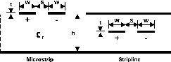
As the stamp cards are quite small, the traces on these boards stay short by construction. Nevertheless, the differential traces have to be routed differentially. The traces at the roof board have to be adjusted to the wave impedance of the cable going to the back end. This implies that the two traces have to be parallel and close together and have to have the same length. Depending on design of the differential pairs - micro strip or strip line - the differential impedance calculates by [23]
 and
and
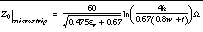 and
and
 |
Furthermore, additional reflections have to be limited by
| end cap |
The front-end electronics of the end cap is split into several equal parts. A wheel is divided into 96 sectors in azimuthal direction and two in axial direction for wheel type A and C - the front-end boards of wheel type B are not split in axial direction. Thus, the outer radius of a wheel holds 192 electronics stacks (type A and C, 96 for type B). Each stack consists of two boards - the ASDBLR board and the DTMROC board containing different numbers of ASDBLR and DTMROC chips according to the number of straws of the different wheel types. For example for wheel-type A, the ASDBLR board contains eight ASDBLR chips and the DTMROC board four DTMROC chips, leading to 64 channels per stack.
Different intermediate "roof" boards are currently used because of the characteristics of the old version of the ASDBLR and the DTMROC chips. When the final chips will be available, a solution like in Figure 2.18 is envisaged. The data comes from the web from the bottom travels through the ASDBLR board to the DTMROC board. At that level the data from three different DTMROC boards is gathered together on one single DTMROC board to leave the front electronics over a common cable bundle.
As in the barrel, it is essential to keep the traces from the straw to the ASDBLR and from the ASDBLR to the DTMROC as short as possible which is mainly provided by the small geometry. The LVDS lines from the DTMROC have to be handled as on the roof board of the barrel. They have to be distributed as differential micro strip or strip lines adjusted to the wave impedance of the cable.
Since the space in the inner part of the detector is confined and the amount of introduced material has to be as low as possible, very thin cables have been designed and tested. Though these cables can be used up to a length of 10 m, they are much more expensive than thicker cables. Therefore they are only used for the first meters to an active repeater patch panel in the calorimeter gap.
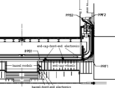
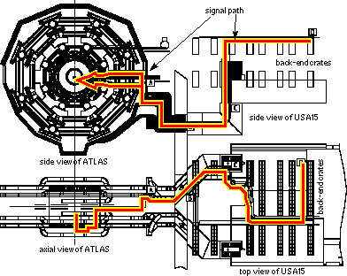
The cables from the barrel run from the abutting face of the barrel up to the cryostat wall along the cryostat wall to the end of the end cap and up to a gap in between the front-end crates of the calorimeter where the repeater patch panel (PPB2) is situated. The cables of the end cap follow the cryostat wall to the last wheel and further outside to the patch panel (PPF2) in the calorimeter gap. Intermediate patch panels (PPB1, PPF1) are introduced into these paths to facilitate the assembly - see Figure 2.19.
 |
As the data-signal read out is handled in longitudinal direction and the timing and control signals are distributed in azimuthal direction - see Chapter 2.1.7, the cables coming from the detector have to be regrouped in the cable trays up to PPB1 and PPF1 - see Chapter 2.1.5.
| cable |
The currently chosen cable is a custom-made shielded twisted pair (STP) by a swedish company called Habia3. The AWG36 cable consists of two individual silver-plated copper conductors of 130 um diameter and a wrapped aluminum-polyester foil as shield. Four drain wires provide a solderable electrical contact to the aluminum shield. The insulation is a special radiation-hard silicone polyetherimide copolymer. The published electrical properties from the manufacturer are a wave impedance of 96 Ohm, a capacitance of 55 pF/m and an attenuation of 0.55 dB/m.
These values where confirmed by measurements with a LANTEX PRO XL cable tester [31]: a wave impedance of 92.5 Ohm; an attenuation of 6 dB at 40 MHz and of 8.9 dB at 100 MHz for 10 m; a propagation time of 5.3 ns/m; a capacitance of 57 pF/m; and a DC resistivity of 1.4 Ohm/m.
The small size of the cable represents a problem in terms of mounting the cable to a connector. The small cable and especially its shield can not be terminated with standard industrial procedures. The proposed solution is to hand solder the cable to an intermediate board which holds the connector.
| intermediate patch panel |
The intermediate patch panels at PPB1 and PPF1 have to provide a demountable interface for the assembly of the detector. They are made of two small PCB boards holding the connectors and the cables.
| signal transmission |
Though twisted-pair cables are used for decades, no uniform solution exists to calculate the characteristic properties of twisted pairs not to mention shielded twisted pairs. Several approaches exist for limited applicability, e.g. [32] to [34], but they mostly neglect the frequency dependence. Furthermore, for the small diameters like in this case not only the skin effect but also the proximity effect has to be included into the calculations.
The maximal length from the farthest front-end electronics to the calorimeter gap is about 8 m. Thus tests with cable samples of 10 m length have been carried out to measure the signal integrity.
A special bit-error-rate tester (BER tester) has been designed [35]. It makes it possible to test four bundles of 20 signal pairs. The board consists of separate driver and receiver circuits for sending and receiving LVDS signals. Random or periodic data can be generated at rates up to 80 Mbit/s with different voltage swings.
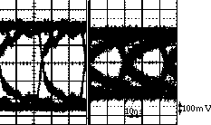
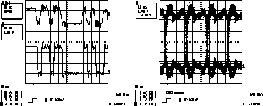
A bit-error rate below 10 -13 has been measured for data transmitted at a rate of 40 Mbit/s. This ensures the required transmission rate of 40 Mbit/s over 8 m. Other measurements have shown that the use of these cables with LVDS drivers and receivers does not introduce any significant degradation of the timing accuracy: less than 180 ps jitter is observed on a 40-Mbit/s signal over 10 m of cable - see Figure 2.21.
To ensure signal integrity on the intermediate patch panels, the differential impedance of its traces has to be matched to the wave impedance of the cable - see above (2.12) to (2.15).
 |
| signal transmission |
In terms of signal integrity, the repeater consists mainly of three parts: the differential PCB traces from the input connector to the repeater and from the repeater to the output connector, the termination of the incoming signal, and the actual repeater - see Figure 2.22.
The differential impedance of the PCB traces has to be matched to the wave impedance of the incoming and the outgoing cables using the formulas (2.12) to (2.15) given in Chapter 2.1.3 which is about 100 Ohm - in fact 92 Ohm for the incoming cable from habia - see SChapter 2.1.4 - and 100 Ohm for the outgoing cable - see Chapter 2.2.4. The routing has to obey the same rules as the front-end boards - see Chapter 2.1.3.
A single resistor of about 100 Ohm terminates the differential transmission line as close as possible to the input pins of the repeater chip. The termination for the common mode is situated at the driver side. Two resistors of 100 Ohm were placed as close as possible to the DTMROC from the output pins to a reference voltage and a capacitor of 22 nF to ground.
| repeater |
The repeater has to reshape the incoming LVDS signal which is deformed by the attenuation and dispersion of the cable - see Figuer 2.21. To achieve this, we tested several solutions:
 |
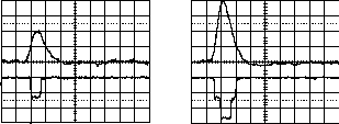
The third solution is based on the idea of skipping the intermediate TTL signal to reduce electromagnetic interference - see Chapte 3. The signal is repeated directly from LVDS to LVDS without transforming it to TTL. Several concepts based on the ultra-high-frequency transistor array HF3XXX from Harris Semiconductors7 which contains 15 NPN transistors, 11 PNP transistors, and 4 FET transistors and allows custom metallization [36] have been designed and simulated (e.g. see Figure 2.42 and Figure 2.23).
However, this solution had to be abandoned due to a minimum production cost of 500,000 DM [37].
Therefore I designed two different multi-layer repeater patch panels [38] according to the old requirements using for the first the LVDS receiver DS90C032 and the LVDS driver DS90C031 and for the second the fast comparator MAX901 and the LVDS driver DS90C031 - see Figure 2.24.
 |
Before the production I completely simulated the boards with a signal-integrity tool called SpectraQuest from Cadence8. There occurred no problems in terms of reflections for the differential traces which I designed according the above mentioned rules - the traces are matched to the wave impedance of the cables and cross the layers only where it is really necessary, and the termination resistor is placed close to the receiver. The simulations pointed out reflections for slow-control TTL signals, but they were solved by termination of these lines. However, the final version of the DTMROC will not need this kind of signals.
Measurements and tests with the real PCB boards confirmed the design and the simulations.
A bipolar ASIC for the final version of a repeater chip will be designed, first to remove the intermediate TTL signals and second to minimize the size, as the complete receiver will be housed in one single package.
| re-grouping |
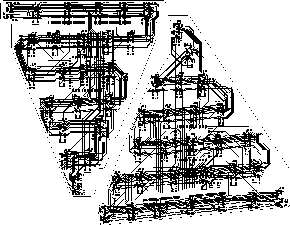
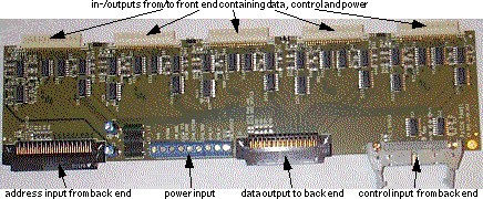
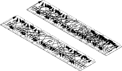
The design of this small patch panel showed that even for a small number of channels six layers were needed to distribute all - data and control signals and power - over one single board even when no regrouping was necessary. Figure 2.25 shows a space estimation of a repeater patch panel with the old requirement of regrouping. This leads for 1/32 of the end cap to two patch panels of a length of about 70 cm. A further splitting of the board is not possible due to the granularity of the readout and control regions. The arrows in the picture indicate the traces which have to go from one connector over a repeater to the other connector. Routing this board would mean to create a high-density PC board with multiple vias to cross the different layers and thus adding reflections.
Thus the regrouping was shifted to the cable tray between the front-end electronics and the first patch panel. This creates a complex cable bundle with multiple connectors at the front-end side and multiple connectors on the patch-panel side, but it allows to replace the two big complex boards by several separate small simple repeater patch panels for data, control and power distribution - see Figure 2.26.
 |
The traces become short and straight and do not have to cross layers even when only a four-layer board is used.
 |
The high attenuation and costs exclude the use of the same small custom cable as is used for the way from the TRT to the repeater patch panel. It is intended to use a standard cable of a thicker diameter without individual shielding (UTP). The current candidates are multi-conductor twisted pair cables of AWG28 from the German company Wächter and the American company Montrose9. An overall shield consisting of a copper braid and an aluminum foil surrounds 27 of the individual twisted pairs.
 |
| signal transmission |
The LVDS standard is actually a high-speed transmission standard for a cable length up to maximal 10 m. It is specially designed for small electromagnetic interference. Never before has it been used for a transmission length of 100 m. Therefore special care is needed for the transmission from the repeater patch panel to the back-end electronics.
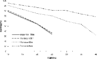
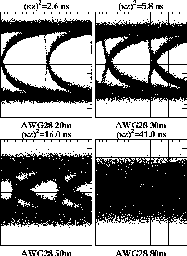
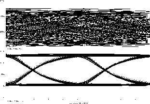
Tests carried out in 1997 before I arrived at CERN indicated that a sole use of these cables does not provide signal integrity at all - see Figure 2.29. Cables of different lengths were investigated at data rates of 40 Mbit/s. Their eye plots show a rapid degradation of the signal with increasing cable length. This limits the usable length to about 40 m. Longer cable runs require either a repeater, a compensation network, or a better cable.
 |
One of my first tasks at CERN was to characterize new samples from Wächter and Montrose of lengths of 60 m, 80 m, and 100 m. The results were comparable to the previous samples. An error-free transmission of LVDS signals with a bit rate of 40 Mbit/s is only possible up to a cable length of 60 m. The eye opening for longer cables is too small to achieve this transmission rate - see Figure 2.30.
 |
The individual twisted pairs must have different numbers of twists per meter to achieve low cross talk in multi-conductor cables. Furthermore, they are not running straight inside the bundle but are twisted against each other. This improves the properties of the mechanics and the EMC of the cable but results in differences in the length of the individual twisted pairs. The maximal measured signal-delay difference between two pairs of the same cable bundle was 18 ns after a transmission of 100 m - see Figure 2.31. This translates to differences in the length of the individual cable of up to 3 m which corresponds to the given tolerances of the manufacturer of 3%.
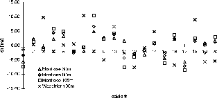 |
Figure 2.31 shows that the length differences result from the manufacturing process. The three cable bundles from Montrose descend from the same lot and have the same pin out on their connectors. Thus, the deviation of the length of the individual pairs in the 60-m cable is related to the 80-m cable and the 100-m cable. This problem is solved in the back-end electronics by synchronizing each single input separately - see Chapter 2.1.7.
| cable model |
As indicated in Chapter 2.1.2, no coherent approach exists to model twisted-pair cables. Nevertheless, a cable model is essential for the derivation of a proper compensation network.
The SCT group suggested in [25] a solution derived from [41]. It describes the output of the twisted pair with a step function a the input by the complementary error function

 .
.
 |
The simulation of the eye plots for 20 m, 30 m, 50 m, and 80 m show a clear accordance to the measured data - compare Figure 2.29 and Figure 2.32.
 |
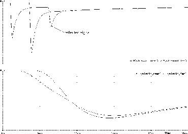
Using the model to calculate the Heaviside response hTi of a 100-m-long cable shows significant deviations from the measured real signal - see Figure 2.33. However, it is an approximation derived for high-frequency signals and thus the obtained response is accurate only when the pulses are short.
A more realistic approach is to develop a frequency dependent R'G'L'C' model.


 .
.
The same problem exists for commercial simulation products like Maxwell from Ansoft10 which are able to simulate variable skin depths by eddy-current methods for quasi-static applications but assume that this is only valid for the conductor losses. The frequency dependency of the inductance is neglected. The high-frequency field solvers even define all currents as surface currents and calculate frequency-independent values.
Normally it is enough to get a simplified model of a cable to match a compensation network as the described deviations have only small effects. But with increasing length the small pieces sum up and are not negligible any more when the signal operates in the intermediate frequency range where these effects matter.
However, to define a compensation network for the cable, a more practical approach was used. I sampled carefully the step response hT(tT) of the 100-m-long cable with specially constructed probes. Into the sampled response, I fitted a simple exponential function


 .
.
 |
This approximate transfer function of the cable determines a rough filter which has to be tuned in PSpice by using models of piece-wise-linear functions of the measured step response hT(tT) , a single pulse with a width of 25 ns
 ,
, .
.| compensation network |
The compensation of the signal distortion can take many forms. For many low-frequency circuits, it often uses a combination of active and passive components to create frequency selective filters that provide specific amounts of gain or attenuation. At higher operating frequencies, the design and implementation of active filters becomes more difficult, and equalization is usually performed using only fixed passive components, followed by a non-frequency selective amplifier. Thus a simple balanced bridged-H equalizer was chosen - see Figure 2.35. It has to attenuate the low frequency part of the incoming signal and to terminate the cable properly.
 |
The filter is adjusted to appear across a wide frequency range as resistance without reactance. For frequencies at or near DC, the insertion loss is determined only by the resistors. As the frequencies approach the active region of the filter, the reactive nature of the capacitors starts to have an effect. The higher frequencies see less reactance and are passed through the capacitor with minimal attenuation. The inductor is selected to exactly match the frequency response characteristics of the capacitors.
R1 is determined by the characteristic impedance of the cable:

 .
.
 ,
,
 |
The simulation of the filter agreed with the measurements of the realized filter - see Figure 2.36 and Figure 2.37. The jitter is limited to less than 2 ns but also the amplitude of the differential signal is attenuated to about 120 mV.
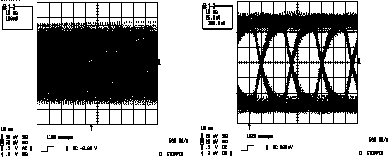 |
The bit-error-rate tester was modified to validate the cable filter. Only the bit error rate of one single twisted pair could be measured due to the different length of the individual pairs inside a cable bundle which increased the test time dramatically. However, the test was running for 812 hours with a data rate of 40 Mbit/s thus transmitted 117 Tbit without showing any error. This proved the BER to be smaller than 10 -14 .
 |
 |
To be able to handle the enormous data stream of more than 1 Tbit/s, the TRT is split into special regions of interest (ROI) - in sectors of 1/32 of the TRT seen in Figure 2.39. The readout is organized in subsets of this regions. One ROD will handle 1/96 of each end cap. For the barrel one ROD will read out 1/32 of each barrel side. It gives a total number of 128 identical RODs per side of the detector and 256 for whole TRT.
| signal integrity |
The important part for the integrity of the signal sent from the front-end electronics is the read-out section of the ROD.
The channels of 104 DTMROCs read-out by one ROD receive the trigger-accept signal (L1A) at the same time. But as they are spread all over the detector surface and the start of the data output is not precisely defined, and because of different cable lengths and transfer propagation times in components described in Chapter 2.1.6, the data will arrive with different phases from the various parts of the front-end electronics. So the data is event but not clock synchronized. The phase difference can reach up to three clock cycles due to the different start of the data output of the DTMROCS, about 20 ns for different cable lengths due to the detector dimensions, and up to 20 ns for the different cable lengths inside a cable bundle. Thus the clock phase of each input line has to be adjusted in order to get a proper sampling window for the data and the event phase in order to synchronize the data.
For the phase adjustment, the ROD contains a phase measurer which allows one to choose either the rising or the falling edge of the ROD clock to strobe the data in the input synchronization circuit. This rather crude delay is sufficient when the input data is guaranteed to be valid for more than 12.5 ns. The phase measurement should be performed once in a while to check the phase stability.
For the event synchronization, the ROD is able to detect the preamble "101" at the beginning of the header of the data from the front-end electronics within a event-phase shift of five clock cycles.
Before synchronizing, the data has to be recovered from the incoming distorted LVDS signal. The compensation network attenuates the LVDS signal to about 110 to 120 mV peak to peak. Tests showed that all examined standardLVDS receivers (DS90C032, DS90LV032A, MNDS90C032-X, and SN65LVDS32 - see Chapter 2.1.5) are able to detect the signal with the requested bit error rates although their data sheets specify a minimum differential voltage of ± 100 mV. Thus an error-free signal transmission would only be guaranteed when all receivers are tested before. In addition, a high detection-threshold causes an increased jitter of the signal. Therefore bit-error-rate tests showed a small sampling window of less than 9 ns.
Using instead of the commercial LVDS receivers the fast comparators MAX901 and MAX964 with a much lower threshold increases the sampling window up to 18 ns - see Figure 2.40.
 |
The termination and routing of the differential signals on the ROD board have to follow the guidelines given in Chapter 2.1.5.
| February 9, 2000 - Martin Mandl | Copyright © CERN 2000 |
 represents the loss angle of the dielectric.