| CERN -> ATLAS -> TU Vienna | ||
|
High-Density Digital Links | |
| LVDS transmission |
The LVDS driver stage consists of a current source which drives one of the differential lines and sinks the same amount of current from the other line. Noise from the environment appears on both lines equally and thus is rejected by the receiver which looks at the difference between the two signals. The electromagnetic field of the transmitted signal is concentrated between the lines which reduces the radiation to the outside world. Thus the signals and the transmission line have to be balanced.
However the fall time of the signal is faster than its rise time. Introducing an additional capacitance between the lines decreases the slew rate and thus the skew between rise and fall time. It can be shown [54] that the stray capacitance of increased IC pads is enough to produce this effect. Though, a higher capacitance and thus lower slew rates provide lower noise to the environment.
| repeater |
The repeater patch panels are situated close to the most sensitive part of the system - the LAr calorimeter and its front-end electronics. Thus the repeater should be as quiet as possible.
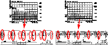
Measurements of the magnetic near field of two prototypes of the repeater patch panel - see Chapter 2.1.5 - indicated much higher stray fields for the digital LVDS receiver DS90C32 than for the analogue comparator MAX901. The boards use the LVDS receiver or the comparator to generate a TTL signal which feeds a LVDS driver to regenerate the LVDS signal. The layouts of the boards are practically identical but the different pinout of the LVDS receiver and the comparator. The different radiation descends from the different technologies - bipolar versus CMOS. The measured fields are concentrated around the repeaters for the control signals which include the 40-MHz clock. However, they are not measurable 10 mm above the board. The new analogue chip - to be designed - will further reduce the noise level by removing the intermediate TTL signal.
| cable |
For the first meters from the front-end electronics to the repeater patch panel, the transmission is carried out over individually shielded-twisted-pair cables of AWG 36. The twisting reduces the inductive coupling and together with the balanced transmission capacitive coupling. The shield - beside shielding - concentrates the electromagnetic field and helps to balance the cable parameters. Further outside from the repeater patch panel to the back-end electronics, bundles of 28 twisted-pair cables share a common shield. Different twist lengths among the cables reduces the cross talk inside a bundle.
Measurements in collaboration with LAr [55] and SCT [25] showed no significant influence of the cables to their environment.
For low voltage the modularity is 1/32 of each barrel module and each end-cap wheel. This gives a granularity of 1,344 independent modules. Each of these modules has its own power supply for 5 V and for ± 3 V.
An even higher modularity is available for the high-voltage supply of the straws. One supply is connected to only 64 straws (on average), which gives a total number of 6,272 independent high-voltage supplies.
| low voltage |
The LV lines can introduce noise picked up from the environment into the system, but also pollute the system with the noise of the digital part of the front-end electronics. Thus a filter has to stop noise in both directions. Standard applications use for this filter electrolytic tantalum capacitors of some tens of microfarad and inductors with ferrite cores of some micro-henry. The high radiation inside the detector would activate the tantalum. Due to the long half-live time of 114 days [56] of the activated tantalum, it is forbidden to use such capacitors. Fortunately, high-value ceramic capacitors became industrially available in 1999 which allows one to use ceramic capacitors up to 22 uF.
The high static magnetic field of 2 T within the Inner Detector saturates the ferrites of inductors. Commercially available ferrites saturate at 0.7 to 0.8 T. Ferrites with higher saturation are in development but not yet available. Thus only air-core inductors are usable for the TRT-front-end electronics. The maximal value for the small dimensions to fit into the confined space of the front-end electronics is 220 nH.
These would be adequate values to produce a filter with a high insertion loss for high frequencies. However, self-resonance effects due to parasitic serial inductances of the capacitors and their traces- see Figure 3.14 - degrade the filter.
Figure 3.15 shows simulations of the low-voltage filter for the possible component values in different configurations with and without parasitic inductances for a source and a load of 50 Ohm. The parasitic inductances have a considerable effect on the behavior of the filter.
Thus the noise on the low-voltage lines from the digital front-end electronics has to be handled like a data signal. The noise is transmitted over shielded-twisted-pair cables to a low-voltage patch panel at PPB/F2 where a lower magnetic field and more space allows better filtering.
Although it was not part of the base-line design, the analogue and the digital supply preferable will have separate returns and should run in separate bundles.
 |
Within the electronics, decoupling capacitors have to stabilize the supply voltages. They have to be big enough to store sufficient charge to supply the switching chip, but have also to be as small as possible to avoid self-resonance effects. Traditionally, the value of the decoupling capacitor is chosen on the allowed value of voltage drop dU on the power line, the switching current I and the switching time dt :

Using 10 to 22 nF capacitors as decoupling capacitors should be adequate for all the front-end electronics of the TRT.
| high voltage |
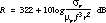
A high-voltage filter - see Figure 3.2 - filters the incoming high-voltage lines. The time constant produced by the filter resistors Rfilter (5 kOhm) and the filter capacitor Cfilter (3 nF) is, at 15 us, a factor 1,000 longer than the 20-ns shaping time of the ASDBLR. This should achieve adequate filtering. In addition, the isolation resistors of 100 kOhm which isolate the different high-voltage groups, act as a noise limiter.
The transmission of the high voltage is carried out from the front-end electronics to the patch panel in PPB/F2 over miniature coaxial cables. At this patch panel it changes to a multi-conductor cable with a common shield.
| component placement |
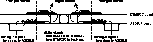
The most likely cross talk within the front-end electronics comes from the coupling of the digital electronics - the DTMROC and the digital part of the ASDBLR - to the sensitive inputs from the straw. Thus they have to be separated in space, so that the return currents of the straw signals do not overlap the return currents of the digital signals. Moving the input connectors with the straw signals to the edges of the board and the output connectors to the middle of the board allows this segregation - see Figure 3.16. Thus the path for the signal return of the sensitive input lines from the straws do not have to share a common impedance of the ground plane with the output signals. In addition, this reduces the length of the signal traces.
| power decoupling |
When a chip is switching, it first gets the needed charge from the local capacitance of the power planes, then from the nearest decoupling capacitor. If these two can not provide the necessary energy in an adequate time, the switching chip affects its environment. To limit this kind of cross talk, each chip or power pin respectively has to have its own decoupling capacitor which is located close to the power pin. Multiple vias - at least two per pin - decrease the serial inductance of the capacitor and limit self-resonance effects.
| power & ground planes |
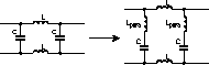
Separate layers with full ground and power planes - see Figure 3.17 - provide additional decoupling capacitance of about 20 pF/cm 2 with very low inductance.
Wether or not split ground planes give better electromagnetic compatibility and signal integrity than continuous planes, depends very much on the layout and circuit design. Split planes work when the different planes are completely decoupled and no signal trace crosses the gap in between. Split ground planes which overlap each other and have thus high capacitive coupling, tend to oscillate. When a signal line crosses the split, the return current can not flow back directly under the trace and has to take the long way round - see Figure 3.18. This enlarges the surface of the loop which is formed by the trace and the return path and causes an increased crosstalk with return currents from other signal traces and with the further environment.
Balanced signals would ideally not need a local return path, but in practice their balance always degrades at some frequency, and so a nearby return path is needed for the resulting common-mode leakage. The planes close to differential traces are a part of the transmission line. A break in such a line means an inhomogeneity and brings further reflections.
As the TRT-front-end electronics has a lot of interfaces between the analogue and the digital part and complete decoupling of split planes would be difficult, it is recommended to use a single solid ground plane.
Additional ground planes heavily connected to each other support the internal ground planes of the chips under the chip surface and act as shield at the edges of the boards.
| routing |
Keeping all traces and especially the sensitive input lines as short as possible reduces the capacitive and inductive cross talk. The differential traces have to be routed in parallel ways and to be kept on the same layer. The distance between the lines and to the plane below has to be adjusted to the characteristic impedance of the transmission line. They should remain on one layer as each via causes a discontinuity and thus reflections.
The input stage of the ASDBLR is a differential amplifier. A dummy line which is connected to the second input of this amplifier and runs along the signal trace gets the same pickup from the environment as the signal trace itself. This noise will be seen as common-mode signal and will be rejected by the differential amplifier.
All these concepts were implemented in a redesign of the former front-end electronics and allow an operation of the electronics with a low-level threshold of 1.5 fC (150 eV) at the level of the ASDBLR noise. The complete setup of analogue and digital electronics shows no significant increase of the noise level compared with the noise level of the bare ASDBLR chip.
 [57]
[57]
 .
.However, 36,096 data lines, 3,072 low-voltage lines, 6,976 high-voltage lines, and 144 pipes for cooling and active gas supply connect to the detector and thus penetrate the shield and degrade the shielding efficiency. The large size of the detector might generate standing-wave effects. In addition, noise from the digital front-end electronics can reflect back to the sensitive straws which would not see this noise without a shield.
To avoid these effects, it is intended to use local nested shields in combination with a over-all faraday shield. Leading all services in conductive cable trays which are heavily connected to the shield will act like a waveguide below cutoff.
| end cap |
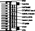
Figure 3.19 shows the physical structure of one half of an 8-plane wheel of the TRT end cap. Three carbon-fibre rings (rings 1, 2, and 3) provide together with two printed-circuit boards (active and passive web) and the straws a self carrying structure which is mounted inside the squirrel cage. The squirrel cage is a cylindrical aluminium cage which surrounds the wheels A and B and holds the cable trays for the services of the end cap. The active web is a rigid-flex PCB with an azimuthal extension of 1/32 of a wheel and connects the straws to the ASDBLR board. In addition, it holds the HV elements like the decoupling capacitors and the isolation resistors. The manifold of the active gas is closed at the top at ring 3, at the bottom of the straws with the inner seal and on the sides of the wheel by a copper-kapton sheet.
The inner seal is a kapton foil plated with 8 um of copper. Together with the inner carbon-fibre ring, this provides a local shield around the straw ends which are opposed to the SCT front-end electronics.
The outer carbon-fibre rings build together with the active and passive web a shield around the straw inputs. The cooling structure supports the shielding effect between the front-end electronics and the straw.
The ground plane of the DTMROC board provides some shielding effect when all digital components are placed and routed above this plane.
The horizontal copper-plated kapton sheet provides a shield in axial direction, though it will be only 500 Å thickness of copper.
The squirrel cage would be an ideal candidate for a over-all shield. Its 6-mm thickness would provide even adequate absorption loss. However, it is littered with openings for the services for the detector and only situated at the outer radius of wheels A and C and even completely missing for the wheels C. Thus a 50-um-copper foil will cover the complete end cap or subsets of wheels respectively.
The number and the size of the shield openings and the way how the services penetrate the shield will influence its effectiveness. A conductive cable tray - strongly connected to the shield - acts as a feed-through capacitor ar waveguide below cutoff for the services - see Figure 3.20. The services enter the shield/cable tray from a common point and have a high capacitive coupling to the shield, while they are running inside the cable tray. This provides effective filtering if afterwards the services enter into the inside of the shield and are not released to the outside.
| barrel |
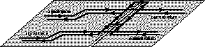
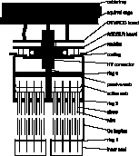
Figure 3.21 shows the physical structure of a barrel module. A carbon fibre structure (shell) surround each module. It is closed at its ends by the electronics boards. The HV board provides the high voltage to the straw. The tension plate connects to the wires and holds small stamp boards with the ASDBLR and the DTMROC. The last board is the roof board which gathers all the data from the DTMROC boards and transmits them to the back-end electronics. The cooling plate is placed between the tension plate and the ASDBLR boards.
The design of the TRT barrel only includes an over-all faraday shield. However, the cooling plate provides, together with the ground plane of the tension plate, a shield between the straws and the front-end electronics. For the over-all faraday shield, it is intended to cover the outer wall of the shell of the outermost module and the inner wall of the shell of the innermost module with a 50-um-copper film. A special ground plane on the roof board shall build the head faces of the shield.
The details of this design are very delicate and are not entirely known yet. It will be quite difficult to connect the single roof boards to each other and herewith to provide a seamless connection. In addition, the shield will have multiple openings for the services of each module. It is recommend to add an additional copper foil on top, as in the end cap, to achieve the same advantages.
Two recent design changes in the barrel electronics could have major impacts on the current shielding design. It was suggested to use a flexible-rigid board holding both, the ASDBLRs and the DTMROC, instead of two individual stamp cards. This shifts the cooling plate into the space between the ASDBLR and the DTMROC part of this board. Thus the cooling structure provides shielding between the analogue and the digital electronics. Second, a flexible-multiple-bent circuit will replace the rigid roof top. Therewith, the over-all shield cannot be closed any more in the intended way.
| February 9, 2000 - Martin Mandl | Copyright © CERN 2000 |